1. Documentation
  2. All
  3. Aironet Developer Platform
Aironet Developer Platform
  • Cisco Aironet Developer Platform Quick Start Guide
    • About Aironet Developer Platform
      • Development Process
      • About This Guide
    • Module Development Guidelines
      • Module Connectivity
      • Constraints
      • Design and Installation
    • HDK Block and Power Diagrams
      • Block Diagram
      • Power Diagram
    • HDK Elements
      • Specifications At-A-Glance
      • Ethernet
      • I2C/SMI Address Assignments
      • MAC Address Assignments
      • Serial IDPROM
      • Power and I/O Interfaces
        • Power and I/O Ports
        • Onboard Power Supplies
        • Power Input
        • Power Output
      • Signal Header and Control Pins
        • Ethernet Addresses and Signal Header Connections
        • Golden Finger Connector Pin Assignment
        • Headers and Control Pins
        • Power I/O Control
        • Sensor Control Pin
      • LED Indicators
    • HDK Mounting and Installation
    • Single Board Computer Support
    • WLC Configuration
    • Additional Resources
      • IVT & Compliance
    • Community and Support
      • Developer Support
      • FAQs

Power and I/O Ports

Figure 8: HDK Ports - Top View

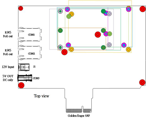
Figure 9: HDK Ports - Bottom View

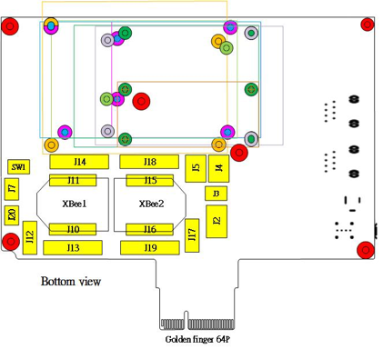
The ports are as follows:

  • Ethernet Ports (RJ45):
    • CON1: Ethernet Only
    • CON2: Ethernet with PSE output
  • DC Jacks:
    • J1: 12VDC input as supplemental power for the HDK
    • J5: 12VDC output for application module (limited to 18W minus HDK loads)
  • USB port:
    • CON3: USB Type-A connector providing 5VDC @1A power out
  • PCI 64P Golden finger connector for connecting to the host access point.
  • Pin Headers:
    • J2 ( 12): Application module configuration for Intel, BBB, and Raspberry Pi.
    • J3 ( 11): Reset functionality swap pins.
    • J4 ( 8-10): I2C selection and UART/I2C control pins.
    • J7 ( 6): External I2C pins for external sensor usage
    • J8 ( 13): PSE output AF/AT control pin.
    • J9 ( 2): Connector power output enable pins.
    • J10 and J11: XBee module socket.
    • J12 and SW3 ( 5): XBee control pins and 5V/3.3V supply selection for control module.
    • J13 ( 7): XBee module 3.3V power enable pin.
    • J14 ( 4): EM module 3.3V power enable pin.
    • SW1 ( 3): HW reset switch.
    • SW2 ( 1): Connector power output enable switch.
Next