Power I/O Control (HDK Rev1)
Power Switch and Enable Jumper Pin
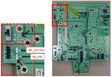
Use the power switch SW2 to set the output power as USB 5V out, PSE out, or 12V out. The location is No. 1.
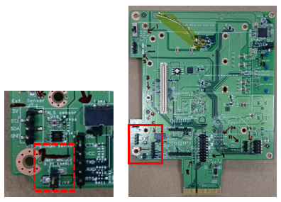
Alongwith using the power switch, use the EN Jumper (J9) enable pin, to enable the corresponding power output port. The location of the jumper pin is No. 2.
The switch and jumper positions are described in the tables and figures below.
| Switch Position | Power Output via Port |
|---|---|
| PSE Out | PSE 54 V output via RJ45 CON1 |
| 12V Out | DC 12 V output via DC Jack J5 |
| USB 5V Out | USB 5 V output via USB CON3 |
| Jumper Position | Power Output Port |
|---|---|
| No jumpers (Default) | USB CON3 output enabled. PSE and 12 V output disabled |
| Put jumper at pin-1, pin-2 | PSE 54 V output enabled |
| Put jumper at pin-3, pin-4 | DC 12 V output enabled |
Figure 29: Jumper Positions on J9 Enable Pins
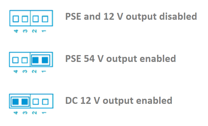
Figure 30: EN Jumper and Power Switch (J9 1*4P 2.54 mm, SW2)
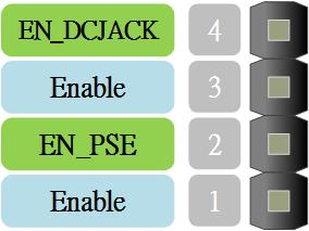
Figure 31: EN Jumper and Power Switch location (No. 1, 2)
EM Module Power Enable Pin
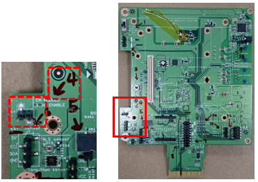
The header J14 is the enable pin for providing 3.3 V power (maximum 6 W) for the EM module. Put on jumper on these pins to supply 3.3 V to the EM module. The location is No. 4.
Figure 32: EM module power enable header (J14 1*2P 2.54mm)
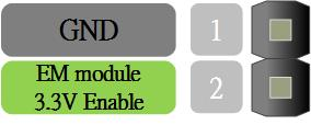
Figure 33: EM module power enable header location (No. 4)
XBee Module Power Enable Pin
The header J13 is the enable pin for providing 3.3 V power for a Digi XBee module. That location is No. 7. Put the jumper on these enable pins to supply 3.3 V to the XBee module.
Figure 34: Power Jumper for XBee Module (J13 1*2P 2.54mm)
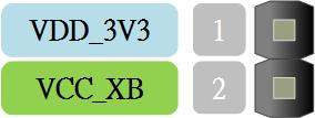
Figure 35: Power Jumper Location (No. 7)